Skip to content
Main Menu
Home
Products
Menu Toggle
Nanoscale Printing System
Printed Sensors
Technology
Menu Toggle
Nanoscale Printing
Overview
Applications
Company
Menu Toggle
News
Team
Vision
Welcome to the future of
Semiconductor manufacturing!
A game-changing technology
Nanoscale Printing of
electronics and sensors
Printing of micro and nanoscale electronics and sensors (down to 20nm).
Prints electronics with a cost saving of 10 to 100 times.
Prints on any rigid or flexible flat surface.
Prints at ambient temperature and pressure.
Prints using any conductive, semiconducting or insulating materials.
Our fully automated printing systems include integrated registration and alignment; annealing and inspection.
New printing wireless sensor system technology.
Patented new printing chemical and biosensor technology.
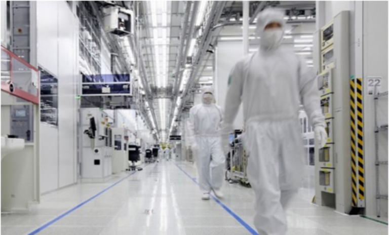
Traditional semiconductor manufacturing challenges
Material choices are extremely limited.
Financial Costs associated with establishing and operating a fab are astronomical ~$20 billion.
Environmental impact of operating a fab is extremely devastating -depleting natural resources.