Innovative R&D enables cutting Edge Technologies for Developing Next-Generation Devices
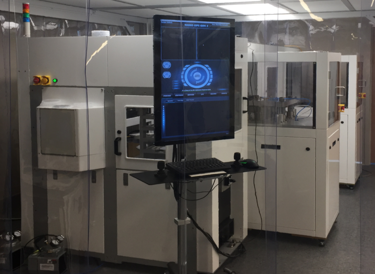
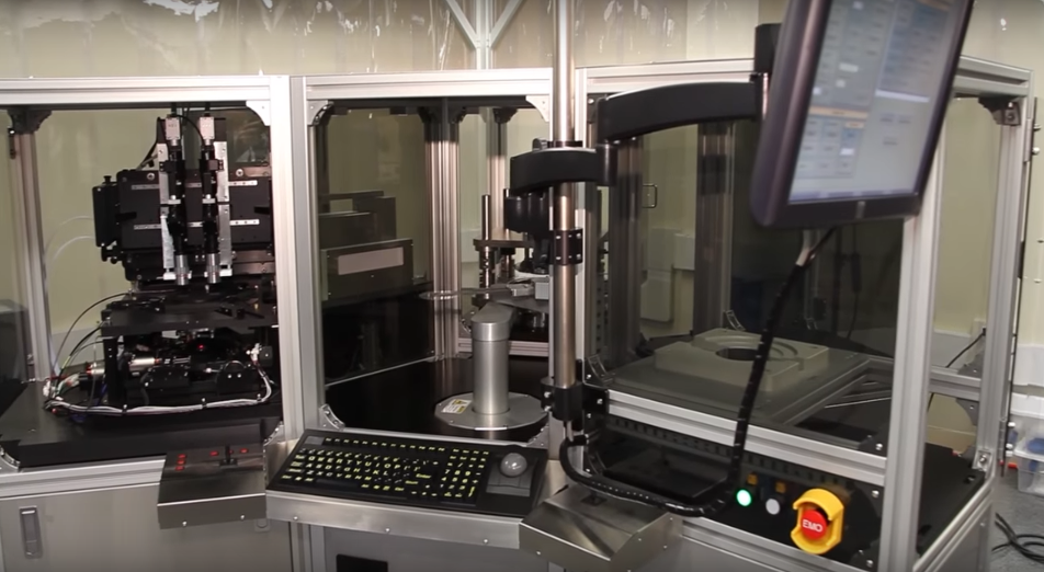
Nano OPS, Inc. has built the world’s first fully automated nanoscale printing system for sensors and electronics. The technology was developed at the NSF Center for High-rate Nanomanufacturing at Northeastern University in Boston, Massachusetts.
The system can print conductive, semiconducting, insulating (organic and nonorganic) materials into nanoscale circuits and structures down to 20 nanometers onto flexible or rigid substrates.
Nano OPS, Inc presents Nano OPS; a disruptive technology for printing nano and micro scale sensors and electronics.
The system can print sensors and electronics 1000 (one thousand) times smaller and 1000 (one thousand) faster than inkjet or 3D printer.
The system costs 10 to 100 times less than any conventional fabrication.
OUR VISION
To “democratize” nanomanufacturing, making it more broadly accessible to industry and entrepreneurs.
Nano OPS printing system eliminates the high cost of entry barriers of nanomanufacturing for small, medium as well as large size businesses.
Nano OPS system is based on over 30 patents that cover the directed assembly-based printing and the many printed applications from wireless sensors, electronics, energy to medical, and drug delivery applications.